- To overcome the limitations of optical microscopes, you can replace the beam of light with an electron beam. This is how it is called electron microscope
- The team at Cornell University used an advanced computational method called letter mapping
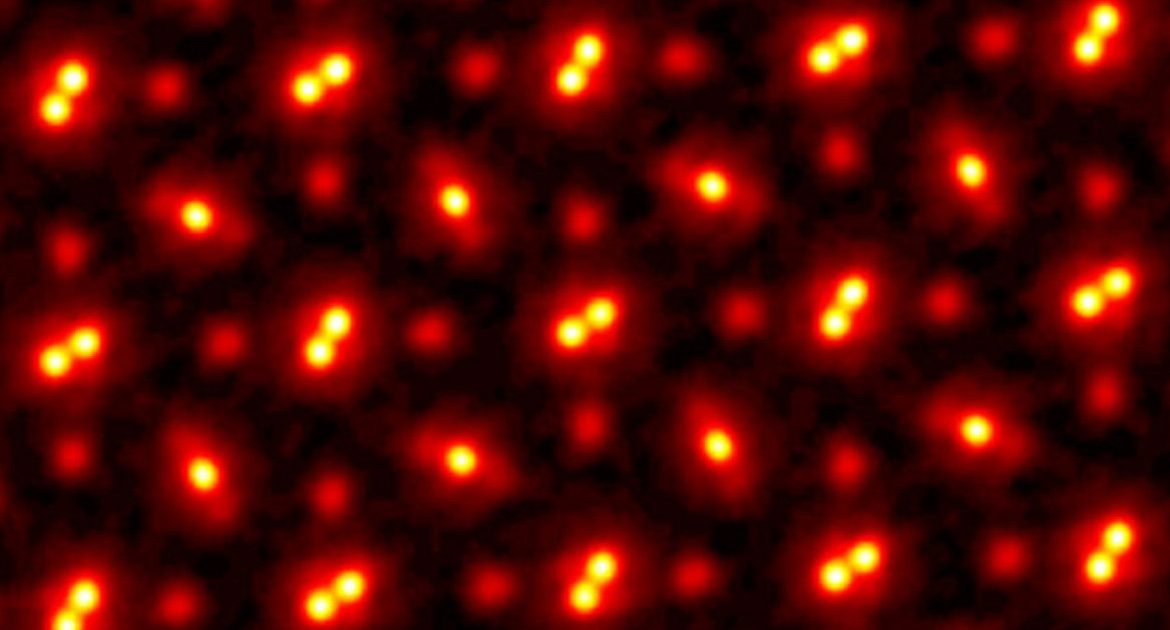
- This led to a single-atom scale sample being photographed, which was entered into the Guinness Book of Records in 2018.
- The current research published in the journal “Science” improves the result obtained then, as it allows imaging of a sample of the material 30 to 50 nanometers wide with atomic resolution.
- The method used here will be of great importance for the development of modern technologies, including the construction of electronic circuits at the atomic scale
- More such information can be found on the home page of Onet.pl
A microscope is a device that magnifies the image of very small things. Thanks to this, it enables direct study of the micro-world. However, conventional optical microscopes have their limitations. The principle of operation of the optical microscope is based on the so-called approximation of geometric optics. At about this point, the light pulses follow fixed paths called rays of light. It is these rays that bend in optical elements such as lenses for example. All students who draw many such refracted rays of light in different types of lenses in physics lessons realize this and recreate images of simple objects on this basis.
However, light is of a wave nature. If we consider a distance scale similar to wavelength, then the approximation of geometric optics is refracted and the wave nature of light cannot be ignored. The wavelength of visible yellow light is about 570 nm (570 nm for short). One nanometer is one billionth of a meter. Therefore, objects that are smaller relative to the wavelength of visible light cannot be seen with a conventional optical microscope.
To overcome the limitations of optical microscopes, you can replace the beam of light with an electron beam. This is how the electron microscope is called. Quantum mechanics teaches us that electrons are particles called a wave function. From the point of view of building electron microscopes, it is important that the wavelength of the electron wavelength is much smaller than the wavelength of visible light. Therefore, the resolution of electron microscopes is greater than that of optical microscopes. This means that by using electron microscopes, you can get a clear image of small objects that are no longer visible with a conventional optical microscope.
Electron microscopy has its limitations, too. The wavelength of the electron’s wavelength is related to their energy. The smaller the wavelength of the electron wavefunction, and therefore the higher the resolution of the microscope, the higher the beam energy. At some point, the power is too high, which leads to a violation of the test sample. To avoid damage to the sample, reduce the power of the package. As a result, on a small enough scale for the tested sample, we must take into account the wave nature of the electrons. Waves can bend over obstacles in the diffraction phenomenon and interfere with the interference phenomenon. These two optical phenomena darken the image in the traditional scheme of microscopes, on a small enough scale.
Instead of fighting the inevitable effects of diffraction and interference, the Cornell University team decided to reconstruct the image of the examined sample on the basis of a properly prepared interference image of the electron beam. For this purpose, use an advanced computational method called ptychography. The use of this method led to the imaging of a sample with a single atomic scale, which was entered into the Guinness Book of Records in 2018. The current research published in the journal “Science” improves the result obtained at that time, allowing imaging of a material sample with a width of 30 to 50 nanometers with atomic precision. The method used here will be of great importance for the development of modern technologies, including the construction of electronic circuits at the atomic scale.
The article was published in collaboration with the Circulation Portal, the Knowledge Portal, and the Social Engagement Portal as part of the Jagiellonian University Strategic Program Excellence Initiative.
(palm)

“Devoted organizer. Incurable thinker. Explorer. Tv junkie. Travel buff. Troublemaker.”